Sep 14-2024
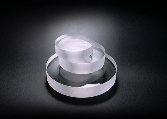
Optical flats serve as primary reference standards for measuring microscopic surface irregularities with nanometer-level accuracy. These precision-grade optical components typically use fused silica or zerodur glass with surface flatness up to λ/20 (≈30 nm deviation). Key applications include:
Interferometric Testing: Monochromatic light interference patterns reveal surface defects, warpage, and flatness deviations on semiconductor wafers, mirrors, and precision-engineered components.
Gauge Block Calibration: Ensures tolerances within ±0.025 µm in metrology labs and manufacturing QA processes.
Lapping & Polishing Validation: Used in optical workshops to verify lens and mirror surface quality before coating.
With low thermal expansion coefficients (≤0.5 x 10⁻⁶/°C), optical flats maintain stability in critical environments like semiconductor fabs and aerospace manufacturing.
Optical flats function as reference planes for aligning high-precision optical system components, including laser cavities, telescopes, and interferometers. Their key uses include:
Beam Steering Verification: Confirms angular alignment accuracy of mirrors and prisms in laser cutting/engraving systems.
Collimator Calibration: Ensures parallelism ≤5 arcseconds in surveying instruments and optical communications equipment.
Fiber Optic Alignment: Used to align fiber end faces in telecom and photonic integrated circuits (PICs) with sub-micron precision.
For high-power laser applications, wedged optical flats prevent back reflections that could damage sensitive equipment.

Optical flats provide non-contact measurement solutions for surface quality verification in mass production:
Automotive Bearings & Gears: Checks flatness deviations ≤0.1µm in transmission components to reduce friction and wear.
Aircraft Engine Turbine Blades: Verifies aerodynamic surface conformity during CNC machining and post-polishing.
Medical Implant Manufacturing: Ensures biocompatible metal/dental implant surfaces meet ISO cleanliness standards.
Advanced versions with anti-reflective (AR) or conductive coatings integrate into automated inspection systems for real-time production monitoring.
Measurement Procedure
Cleaning: This is the most critical step. Thoroughly clean the working surface of the optical flats and the surface of the workpiece to be measured with alcohol and a lint-free cloth (such as lens tissue). Any tiny specks of dust or fibers can create unusual interference fringes, leading to false readings.
Placing: Gently place the cleaned optical flat on the surface to be measured. Typically, one edge of the flat touches the surface first, then gently press down on the other side, like "laying down a piece of paper," to avoid impact. This creates a very thin wedge of air between the two.
Illumination and Observation:
Observe the optical flats from above under monochromatic light.
To see the fringes more clearly, it may be necessary to slightly adjust the viewing angle or gently press on different locations of the optical flats.
Interpreting the fringes: Observe the resulting interference fringe pattern. This is the core of measurement.
With shrinking chip architectures, optical flats are now vital in wafer fabrication and nanoscale metrology:
EUV Lithography Mask Inspection: Detects sub-nm defects on photomasks for 3nm/5nm node chips.
Atomic Force Microscope (AFM) Calibration: Provides traceable flatness standards for probe-based measurements.
Quantum Computing Optics: Ensures wavefront uniformity in superconducting qubit readout systems.
As semiconductor tolerances tighten, optical flats with superpolished surfaces (Rq < 0.5nm) are becoming essential in next-gen chip manufacturing.
From nanotech R&D to large-scale industrial QC, optical flats deliver unmatched accuracy, reliability, and versatility in surface measurement. As new ultra-flat materials like silicon carbide (SiC) and synthetic diamond emerge, expect even higher precision applications in photonics, space optics, and quantum technology.
For manufacturers requiring sub-micron tolerances, investing in certified optical flats ensures compliance with ISO, MIL-PRF, and ASME standards—making them a crucial asset in precision engineering.