Mar 26-2026
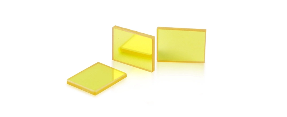
We can process codes, phase gratings, projection gratings, reflective gratings, subdivisionplates, resolution plates and other products on the polished substrate surface of infraredmaterials according to customer requirements.
| Technical Requirement | Tolerance |
| Minimum line width | 1.5um |
| Maximum area | 1 80mm |
| Image tolerance | +0.5um (Based on photoetching area) |
| Depth | 0.05um-10um (Based on width of image) |
| Depth tolerance | 0.001 um |
| Substrate | Si, Ge, Znse, ZnS and othe infrared material ect |
| We can process codes, phase gratings, projection gratings, reflective gratings, subdivision plates, resolution plates and other products on the polished substrate surface of infrared materials according to customer requirements. | |

High Precision Patterning: Infrared lens photolithography offers precise patterning capabilities, crucial for manufacturing advanced infrared devices.
Infrared Transparency: High transmittance in the infrared spectrum enables accurate imaging and patterning.
Durable Construction: The infrared optical components are resistant to mechanical stress and environmental factors, ensuring long-lasting performance.
Broad Spectral Range: Transmits wavelengths from near-IR to far-IR, suitable for diverse photolithography applications.